Friday, December 13, 2013

INPUT/OUTPUT ARCHITECTURE


Input/Output Devices


I/O CAN BE CHARACTERIZED BY
::behaviour; input, output, storage
::partner; human or machine
::data rate; bytes/sec, transfer/sec

I/O bus connection


iNPUT/oUTPUT MODULE

  • Interface to CPU and Memory
  • Interface to one or more peripherals
GENERIC MODEL of I/O MODULE
FUNCTION OF I/O MODULES
  1. Control and Timing
  • CPU asks I/O module to check the status of attached device.
  • I/O module tells the status
  • CPU requests for data transfer to I/O module if device is ready
  • I/O module gathers the data and transfer to the CPU
 2.  CPU Communicating
  • Command decoding
  • Data- Exchange between CPU and Module
  • Status reporting - to CPU, since peripherals are slow
  • Address recognition for the devices connected to it
 3. Device Communication
  • May involves command, status information and data transfer
 4. Data Buffering
  • Essential function to overcome speed mismatch
 5. Error Detection
  • Like paper jam, bad data etc.
I/O MODULE STRUCTURE


INPUT/OUTPUT SYSTEM CHARACTERISTICS


  • Dependability
  • Performance measures
dependability


TECHNIQUES OF I/O


Tuesday, December 10, 2013

THE PROCESSOR 2 : PIPELINING

PIPELINING

A pipeline is a set of data processing elements
connected in series, so that the output of one
element is the input of the next one.

Pipeline Logic

---> A clock drives all the registers in the pipeline. This clock causes the
  • CLC output to be latched in the register which provides input to the next stage, and thus making a start of new computation possible for next stage.
---> The maximum clock rate is decided by the time delay of the CLC in the stage and the delay of the staging latch.


PIPELINING ANALOGY

Pipelined laundry: overlapping execution

◦Parallelism improves performance


FIGURE 1

MIPS PIPELINE : Steps in Executing an Instruction

• Instruction Fetch (IF)
– Fetch the next instruction from memory

• Instruction Decode (ID)
– Examine instruction to determine:
– What operation is performed by the instruction (e.g., addition)
– What operands are required, and where the result goes

• Operand Fetch
– Fetch the operands

• Execution (EX)
– Perform the operation on the operands

• Result Writeback (WB)
– Write the result to the specified location

                        PIPELINE PERFORMANCE

---> Assume time for stages is
  • 100ps for register read or write
  • 200ps for other stages
---> Compare pipelined datapath with single-cycle datapath


FIGURE 2

PIPELINE PERFORMANCE (CONT...)


FIGURE 3

PIPELINE SPEEDUP 1

--->If all stages are balanced

◦ all take the same time

◦Time between instructions(pipelined)
 = Time between instructions(nonpipelined)/ Number of stages

--->If not balanced, speedup is less

Speedup due to increased throughput
◦Latency (time for each instruction) does not decrease

Ideally 5 stage pipeline should offer nearly fivefold improvement over the 800 ps nonpipelined time.

PIPELINE PERFORMANCE

Refer to figure 3, the example does not reflect fourfold improvement for three instructions

◦2400/1400 ≈ 1.7

    Add 1,000,000 instructions, each add 200 ps to the total execution time,

             ◦Total execution time = 1,000,000 x 200 ps + 1400 ps
             = 200,001,400 ps

◦Nonpipelined total execution time
= 1,000,000 x 800ps + 2400ps
= 800,002,400 ps

◦Speedup = 800,002,400/200,001,400

              ≈ 4

PIPELINE SPEEDUP 2


FIGURE 4

Critical Path for Different Instructions


HAZARD

---> Situations that prevent starting the next instruction in the next cycle

---> 3 type of hazard are:

Structure hazards
◦A required resource is busy

Data hazard
◦Need to wait for previous instruction to complete its data read/write

Control hazard
◦Deciding on control action depends on previous instruction


STRUCTURE HAZARD


--->Conflict for use of a resource

--->In MIPS pipeline with a single memory

◦Load/store (pipelined) requires data access at the same time
◦Instruction fetch would have to stall for that cycle
  • Would cause a pipeline “bubble”
--->Solution, pipelined datapaths require separate instruction/data memories


◦Or separate instruction/data caches


DATA HAZARD

An instruction depends on completion of data access by a previous instruction
  • add $s0, $t0, $t1 
  • sub $t2, $s0, $t3


FIGURE 5


SOLUTION : FORWARDING (aka Bypassing)

--->Use result when it is computed

◦Don’t wait for it to be stored in a register

◦Requires extra connections in the datapath


FIGURE 6


LOAD-USE DATA HAZARD


FIGURE 7

CODE SCHEDULING TO AVOID STALLS

Reorder code to avoid use of load result in the next instruction

        C code for A = B + E ; C = B + F ;


FIGURE 8

CONTROL HAZARD

--->Branch determines flow of control

  • Fetching next instruction depends on branch outcome
  • Pipeline can’t always fetch correct instruction

           Still working on ID stage of branch


--->In MIPS pipeline

  • Need to compare registers and compute target early in the pipeline
  • Assume, add hardware to do it in ID stage, test registers, calculate branch address & update PC during 2nd stage of pipeline.

SOLUTION 1 : STALL ON BRANCH


---> Wait until branch outcome determined before fetching next instruction


FIGURE 9

Figure 9 shows a pipeline showing stalling on every conditional branch as solution to control hazards.

This example assumes the conditional branch is taken, and the instruction at the destination of the branch is the OR instruction.


SOLUTION 2 : BRANCH ON PREDICTION

---> Longer pipelines can’t readily determine branch outcome early
  • Stall penalty becomes unacceptable

--->Predict outcome of branch

  • Only stall if prediction is wrong

--->In MIPS pipeline

  • Can predict branches not taken
  • When you are right, fetch instruction after branch, with no delay

MORE - REALISTIC BRANCH PREDICTION

--->Static branch prediction
  • Based on typical branch behavior
  • Example: loop and if-statement branches

           Predict backward branches taken

           Predict forward branches not taken


--->Dynamic branch prediction

  • Hardware measures actual branch behavior

        e.g., record recent history of each branch (as taken or untaken branch)

  • Assume future behavior (predict from past behavior) will continue the trend

       When wrong, stall while re-fetching, and update history


BY AINI KHAIRANI BT AZMI

Monday, December 9, 2013

Branch Instruction

BRANCH INSTRUCTION

---> Read register operands

---> Compare operands
      ◦Use ALU, subtract and check Zero output

---> Calculate target address
     ◦Sign-extend displacement
     ◦Shift left 2 pla-ces (word displacement)
     ◦Add to PC + 4
         -Already calculated by instruction fetch


DATAPATH FOR BRANCH


FIGURE 1


Figure shows the datapath for a branch uses the ALU to evaluate the branch condition and a separate adder to compute the branch target as the sum of the incremented PC and the sign-extended, lower 16 bits of the instruction (the branch displacement), shifted left 2 bits.


BRANCH - ON - EQUAL


FIGURE 2

Figure 2 shows the operation of the branch-on-equal instruction, such as beq $t1, $t2, offset. The four steps execution:

1. An instruction is fetched from the instruction memory, and the PC is incremented
.
2. Two registers, $t1 and $t2, are read from the register file.

3. The ALU performs a subtract on the data values read from the register file. The value of PC+4 is added to the sign-extended, lower 16 bits of the instruction (offset) shifted left by two; the result is the branch target address.


4. The zero result from the ALU is used to decide which adder result to store into the PC

IMPLEMENTING JUMP


  • Implement “jump” by concatenating


         – Upper 4-bits of “PC+4”: NextPC[31:28]
         – 26-bit immediate field from instruction
         – Bits 00

{NextPC[31:28], Instruction[25:0], 2’b00}


DATAPATH WITH JUMPS ADDED


PERFORMANCE ISSUE

---> Longest delay determines clock period

           ◦Critical path: load instruction
           ◦Instruction memory
            register file --> ALU --> data memory --> register file

---> Not feasible to vary period for different instructions

---> Violates design principle

           ◦Making the common case fast

---> We will improve performance by pipelining


BY AINI KHAIRANI BT AZMI

Sunday, December 8, 2013

R-format Datapath


DATAPATH FOR R-FORMAT


R type instructions (e.g. ADD $t1, $t2, $t3)

---> steps:

    • Read two registers
        – Register file

    • Perform an ALU operations
        – ALU

    • Write the result into a register
        – Register file

Datapath component

--->Register file

• A collection of registers in which any register can be read or written by specifying the number of register (register address) in the file.  

• Needs a write control signal “RegWrite”.

• How many ports are required?


---> ALU

R- FORMAT INSTRUCTION

  • Read two register operands (each 5 bits)
  • Perform arithmetic/logical operation (6 bits)
  • Write register result (5 bits)


R- FORMAT INSTRUCTION DATAPATH


TABLE 2

Table 2 shows the operation of the datapath for R-format instruction, such as add $t0, $t1, $t2. The operation:

1.The instruction is fetched, and the PC is incremented

2.Two registers, $t1 and $t2, are read from the register file; also RegDst, RegWrite and ALUOp is set.

3.The ALU operates on the data read from the register file, using the function code (bits 5:0, in the funct field) to generate the ALU function


4.The result from the ALU is written into the register file using bits 15:11 of the instruction to select the destination register ($t0)


LOAD / STORE INSTRUCTION

---> Read register operands

---> Calculate address using 16-bit offset

         ◦Use ALU, but sign-extend offset

---> Load: Read memory and update register


---> Store: Write register value to memory


LOAD / STORE DATAPATH


TABLE 3


Table 3 illustrate the execution of load word such as lw $t1, 4($t2) :

1.Instruction is fetched from the instruction memory, and PC is incremented.

2.Value of register $t2 is read from the register file.

3.The ALU computes the sum of the value read from the register file and the sign-extended, lower 16 bits of the instruction (offset = 4).

4.The sum from the ALU is used as the address for the data memory.


5.The data from the memory unit is written into the register file; the register destination is given by bits 20:16 of the instruction ($t1)


BY AINI KHAIRANI BT AZMI

Saturday, December 7, 2013

Logic Design Conventions


LOGIC DESIGN CONVENTIONS


Types of logic elements


---> Information encoded in binary


  • Low voltage = 0, High voltage = 1
  • One wire per bit
  • Multi-bit data encoded on multi-wire buses


---> Combinational element


  • Operate on data
  • Output is a function of input
  • Output only depends on the current input
  • Uses for ALU, multiplier, and other datapath


---> State (sequential) elements


  • Store information
  • State element to store the states
  • Output depends on current inputs and current states 


COMBINATIONAL ELEMENTS


SEQUENTIAL ELEMENTS


Register : stores data in a circuit (use D flip flop)

---> Uses a clock signal to determine when to update the stored value

---> Edge-triggered: update when CLK changes from 0 to 1


The logical operation of the positive edge-triggered D flip-flop is summarized in the table below :


To write new data in the register, we use D flip flop with Write Enable

--->Write Enable:
  • 0: Only updates on clock edge where the output of the register becomes the input itself (Data in register will not change.
  • 1: New data is fed to the flip-flop and the register changes its state

CLOCKING METHODOLOGY


Clocking methodology

  •  Defines when signals can be read and when they can be written
  •  Mainstream: An edge triggered methodology
  • Determine when data is valid and stable relative to the clock


Typical execution:

– read contents of some state elements,
– send values through some combinational logic
– write results to one or more state elements


BY AINI KHAIRANI BT AZMI

Wednesday, December 4, 2013

Building A Datapath

BUILDING A DATAPATH


DATAPATH COMPONENTS


---> Common to all instructions:
          – Instruction memory
          – PC and its update

---> Datapath of R-R type instructions (e.g. ADD $t1, $t2, $t3)
          – ALU
          – Register set

---> Datapath of memory-reference instructions (e.g. lw $t1, offset($2) )
          – ALU (for address calculation)
          – Register set
          – Sign extension unit
          – data memory

 ---> Datapath for a branch inst. (e.g. beq $1, $2, offset)
          – Sign extension + 2bit shifter
          – Reg
          – Adder
          – ALU (zero output)


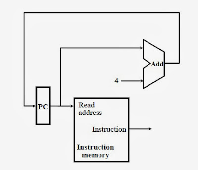
INSTRUCTION MEMORY AND PC UPDATE


Two state elements are needed to store and access instructions and an adder is needed to compute the next instruction address.


PC Datapath and Instruction Fetch

  • NextPC = PC + 4

To execute any instruction, we must start by fetching the instruction from Instruction Memory.

•PC feeds address of current instruction to Instruction Memory.

•Instruction memory read the address and fetch the instruction stored in the memory.

•PC add 4 to hold the next instruction address.


BY AINI KHAIRANI BT AZMI

CPU OVERVIEW AND CONTROL


CPU OVERVIEW


TABLE 1


Table 1 shows an abstract view of the implementation of the MIPS subset showing the major functional units and the major connections between them.


1.All instruction start by using the program counter (PC) to supply the instruction address to the instruction memory. (refer to red line)

2.After the instruction is fetched, the register operands used by an instruction are specified by fields of that instruction.(refer to blue line)

3.Once the register operands have been fetched, they can be operated on to compute a memory address (for a load or store), to compute an arithmetic result (for an integer arithmetic-logical instruction), or a compare (for a branch).

4.If the instruction is an arithmetic-logical instruction, the result from the ALU must be written to a register.
(refer to green line)

5.If the operation is a load or store, the ALU result is used as an address to either store a value from the registers or load a value from memory into the registers.(refer to orange line)

6.The result from the ALU or memory is written back into register file.

7.Branches require the use of the ALU output to determine the next instruction address, which comes either from the ALU (where the PC and branch offset are summed) or from an adder that increments the current PC by 4.

8. The thick lines interconnecting the functional units represent buses, which consists of multiple signals.


MULTIPLEXERS


TABLE 2


In practice, these data lines cannot simply be wired together; we must add a logic element that chooses from among the multiple sources and steers one of those sources to its destination. This selection is commonly done with a device called a multiplexor, although this device might better be called a data selector


DESIGN METHOD FOR CONTROL


--->Multi-level control (decoding)

--->Instruction opcode: main control unit (first level)
        – ALU control

             • Sub-control for arithmetic

       – MUX control
             • Which source registers and destination registers
             • ALU input source
             • Input source of destination register
             • Input source of PC

       – Result for first level
             • Seven 1-bit control lines
             • 2-bit ALUOP control signals
             • The above control signals can be set based solely on the opcode                     field of the instruction
                              # Exception: PCSrc (depends on the beq result)


CONTROL


TABLE 3


Table 3 shows the basic implementation of the MIPS subset, including the necessary multiplexors and control lines.

----> The top multiplexor (Mux) controls what value replaces the PC; the multiplexor is controlled by the gate that “ANDs” together the Zero output of the ALU and a control signal that indicates that the instruction is a branch.

----> The middle multiplexor, whose output returns to the register file, is used to steer the output of the ALU or the output of the data memory for writing into the register file.

----> Finally, the bottommost multiplexor is used to determine whether the second ALU input is from the registers or from the offset field of the instruction.

----> The added control lines are straightforward and determine the operation performed at the ALU, whether the data memory should be read or write, and whether the registers should perform a write operation.


----> The control lines are shown in blue colors.


BY AINI KHAIRANI BT AZMI